555 Timer Schematic Symbol / 24v Flasher Circuit Diagram Using 555 Timer Electrical Technology - The internal block diagram and schematic of the 555 timer are highlighted with the same color across all three drawings to clarify how the chip is implemented:
555 Timer Schematic Symbol / 24v Flasher Circuit Diagram Using 555 Timer Electrical Technology - The internal block diagram and schematic of the 555 timer are highlighted with the same color across all three drawings to clarify how the chip is implemented:. In monostable mode, the duration for which the pin 3 would remain high, is given by the below formulae: One reduces the trigger sensitivity and the other will double the output pulse duration without increasing the values of r1 and c1. May 21, 2020 · the 555 timer. The diagram below shows the actual pin arrangement of the 555 timer with the internal schematic diagram of the ic: The most common use of the 555 timer is to provide timed electrical delays.
For a stable operation as an oscillator , the Capacitor can be used in a timer circuit by adding a resistor. This article covers every basic aspect of 555 timer ic. Jul 14, 2015 · all we need to change the value of resistor r1 and/or capacitor c1. The following schematic shows two additions to the basic 555 timer circuit.
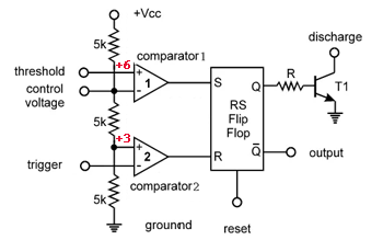
Schematic Circuit Diagram Variable Frequency Pwm Using 555 Timer Proteus Simulation from circuit-diagramz.com This will require a junction. This article covers every basic aspect of 555 timer ic. Capacitor can be used in a timer circuit by adding a resistor. For a stable operation as an oscillator , the As we mentioned above, adding junctions to your schematic allows intersecting nets to share an electrical connection. One reduces the trigger sensitivity and the other will double the output pulse duration without increasing the values of r1 and c1. In this article, we cover the following information about 555 timer ic. Between the positive supply voltage v cc and the ground gnd is a voltage divider consisting of three identical resistors, which create two reference voltages at 1 ⁄ 3 v cc and 2.
May 21, 2020 · the 555 timer.
One reduces the trigger sensitivity and the other will double the output pulse duration without increasing the values of r1 and c1. For a stable operation as an oscillator , the We need to set 555 timer in monostable mode to build timer. A type of variable capacitor is the trimmer capacitor that is small in size. In monostable mode, the duration for which the pin 3 would remain high, is given by the below formulae: This article covers every basic aspect of 555 timer ic. In the time delay mode of operation, the time is precisely controlled by one external resistor and capacitor. The most common use of the 555 timer is to provide timed electrical delays. Between the positive supply voltage v cc and the ground gnd is a voltage divider consisting of three identical resistors, which create two reference voltages at 1 ⁄ 3 v cc and 2. We need to add a net that connects between pin 3 on our 555 timer and our r3 and r4 resistors. To add a junction, you can do it in one of two ways: The internal block diagram and schematic of the 555 timer are highlighted with the same color across all three drawings to clarify how the chip is implemented: This will require a junction.
Capacitor can be used in a timer circuit by adding a resistor. Jul 14, 2015 · all we need to change the value of resistor r1 and/or capacitor c1. This will require a junction. You may already know that se/ne 555 is a timer ic introduced by signetics corporation in 1970's. The following schematic shows two additions to the basic 555 timer circuit.
555 Timer Ic Internal Structure Working Pin Diagram And Description from circuitdigest.com T = 1.1 * r1*c1. We need to add a net that connects between pin 3 on our 555 timer and our r3 and r4 resistors. So to build 1 minute (60 seconds) timer we need resistor of value 55k ohm and capacitor of 1000uf: The following schematic shows two additions to the basic 555 timer circuit. One reduces the trigger sensitivity and the other will double the output pulse duration without increasing the values of r1 and c1. This article covers every basic aspect of 555 timer ic. This will require a junction. Used to vary the capacitance by turning the knob.
In monostable mode, the duration for which the pin 3 would remain high, is given by the below formulae:
May 21, 2020 · the 555 timer. In this article, we cover the following information about 555 timer ic. One reduces the trigger sensitivity and the other will double the output pulse duration without increasing the values of r1 and c1. In the time delay mode of operation, the time is precisely controlled by one external resistor and capacitor. The following schematic shows two additions to the basic 555 timer circuit. Used to vary the capacitance by turning the knob. For a stable operation as an oscillator , the This article covers every basic aspect of 555 timer ic. We need to add a net that connects between pin 3 on our 555 timer and our r3 and r4 resistors. Nand gate conversion & example. We need to set 555 timer in monostable mode to build timer. You may already know that se/ne 555 is a timer ic introduced by signetics corporation in 1970's. To add a junction, you can do it in one of two ways:
As we mentioned above, adding junctions to your schematic allows intersecting nets to share an electrical connection. Nand gate conversion & example. This will require a junction. In the time delay mode of operation, the time is precisely controlled by one external resistor and capacitor. To add a junction, you can do it in one of two ways:
555 Timer An Overview Sciencedirect Topics from ars.els-cdn.com This article covers every basic aspect of 555 timer ic. Nand gate conversion & example. The following schematic shows two additions to the basic 555 timer circuit. So to build 1 minute (60 seconds) timer we need resistor of value 55k ohm and capacitor of 1000uf: In monostable mode, the duration for which the pin 3 would remain high, is given by the below formulae: The notations are all the same. One reduces the trigger sensitivity and the other will double the output pulse duration without increasing the values of r1 and c1. For a stable operation as an oscillator , the
The internal block diagram and schematic of the 555 timer are highlighted with the same color across all three drawings to clarify how the chip is implemented:
To add a junction, you can do it in one of two ways: In monostable mode, the duration for which the pin 3 would remain high, is given by the below formulae: We need to set 555 timer in monostable mode to build timer. Used to vary the capacitance by turning the knob. Between the positive supply voltage v cc and the ground gnd is a voltage divider consisting of three identical resistors, which create two reference voltages at 1 ⁄ 3 v cc and 2. In the time delay mode of operation, the time is precisely controlled by one external resistor and capacitor. As we mentioned above, adding junctions to your schematic allows intersecting nets to share an electrical connection. Nand gate schematic of above function is given below. Jul 14, 2015 · all we need to change the value of resistor r1 and/or capacitor c1. The internal block diagram and schematic of the 555 timer are highlighted with the same color across all three drawings to clarify how the chip is implemented: This will require a junction. The notations are all the same. T = 1.1 * r1*c1.
In monostable mode, the duration for which the pin 3 would remain high, is given by the below formulae: 555 timer schematic. Nand gate conversion & example.


0 Komentar